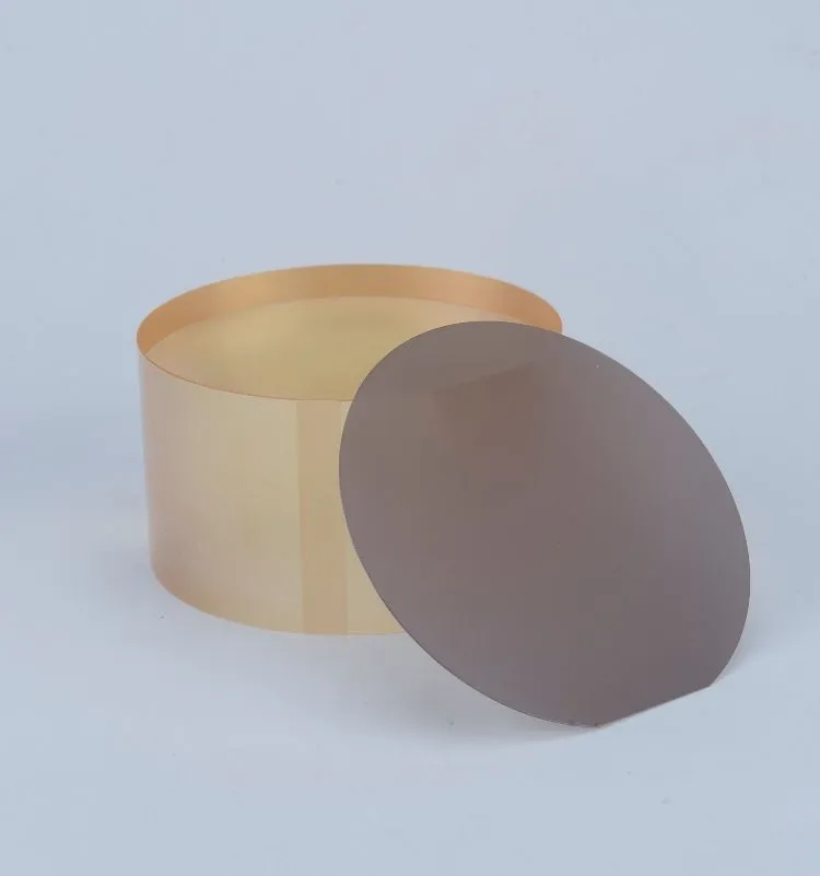
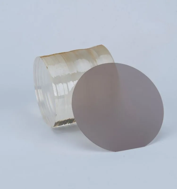
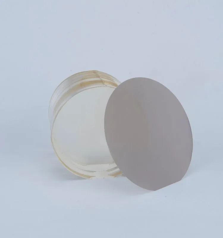
Black Lithium Niobate wafer
Curie Temp: 1142±2.0℃
Cutting Angle: X/Y/Z/Y36/Y41/Y64/Y128/etc
Diameter/size: 3”/4”/6" & 8" LN wafer
Tol(±): <0.20 mm
Thickness: 0.18 ~ 0.5mm or more
Primary Flat: 22mm /32mm /42.5mm /57.5mm /semi notch
The reduction technique is used to produce black lithium niobate (LiNbO3), which has a high ability to neutralize charges even if the electric potential occurs instantaneously. The pyroelectric effect of LN wafer is almost eliminated and the transmittance is significantly reduced. The piezoelectric properties of black lithium niobate wafers are no different from those of standard wafers. Therefore, black reduced lithium niobate wafers are widely used to produce higher frequency surface acoustic wave devices.
Free-pyro black LiNbO3 and LiTaO3 wafers were prepared successfully by chemical reduction under a mixed atmosphere of CO2 and H2. Bulk conductivity and optical transmittance of the black LiNbO3 and black LiTaO3 wafers were measured. The results showed that the pyroelectric effect for the reduced wafers was almost eliminated and the transmittance decreased considerably. The reduction process did not change Curie temperatures or piezoelectric properties of LN and LT wafers, while neutralize electrical charges even if the electrical potential occurs instantaneously.
The reduction technology is used to produce Black Lithium Niobate (LiNbO3) which has high ability to neutralize electrical charges even if the electrical potential occurs instantaneously. Black Lithium Niobate shows no difference in piezoelectric properties from standard wafers. As a result, black reduced lithium niobate wafers are widely adopted to produce higher frequency SAW devices.
| LTV (5mmx5mm) | <1µm | |
| TTV | <3µm | |
| Bow | -30<bow<30 | |
| Warp | <40µm | |
| PLTV(<0.5um) | ≥95%(5mm*5mm) | |
| Surface Type | Single Side Polished /Double Sides Polished | |
| Polished side Ra | <0.5nm | |
| Back Side Criteria | General is 0.2-0.5µm or as customized | |
| Edge Criteria | R=0.2mm or Bullnose | |
| Wafer Surface Criteria | Transmissivity | general:5.9×10⁻¹¹<s<2.0*10-10 at 25℃ |
| Contamination, | None | |
| Particles ¢>0.3 µ m | <= 30 | |
| Scratch , Chipping | None | |
| Defect | No edge cracks, scratches, saw marks, stains | |
| Packaging | Qty/Wafer box | 25pcs per box |
Our Ordering Process
Send us your request with detailed specifications
Receive a commercial offer with terms and costs
After your approval, we handle manufacturing, quality control, and shipping
📦 Shipping
3-5 days in EU, from 10 days to USA
💳 Payment methods
Cash, Bank Transfer, Cards (Visa, Mastercard, Amex, Discover) and PayPal
💬 Questions?
Contact us via WhatsApp, phone, live chat or email


