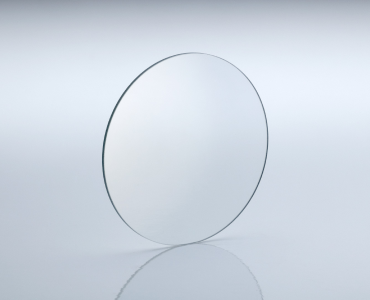
Black Lithium Tantalate
Curie Temp: 603±2℃
Cutting Angle: X/Y/Z/X112Y/Y36/Y42/Y48/etc
Diameter/size: 3”/4”/6" LT wafer
Tol(±): <0.20 mm
Thickness: 0.18 ~ 0.5mm or more
Primary Flat: 22mm /32mm /42.5mm /57.5mm
To produce these reduction wafers, LiTaO3 crystals undergo chemical reduction in a controlled atmosphere. This process effectively eliminates the pyroelectric effect while maintaining the material’s key properties such as Curie temperatures and piezoelectric characteristics.
Lithium Tantalate (LiTaO3) crystals are versatile materials with excellent piezoelectric, ferroelectric, acousto-optic, and electro-optic effects. They find wide applications in resonators, filters, transducers, high-frequency surface acoustic wave (SAW) devices, and bulk acoustic devices.
Specifically, LiTaO3 is favored for both SAW and optical applications due to its substantial electromechanical coupling coefficient and low acoustic attenuation. Typical cut angles for SAW applications include 36°Y, 42°Y, and X-cut orientations. An innovative technology in LiTaO3 production involves reduction processes, resulting in “black” wafers that are devoid of pyroelectric discharge, ideal for high-frequency SAW applications.
To produce these reduction wafers, LiTaO3 crystals undergo chemical reduction in a controlled atmosphere. This process effectively eliminates the pyroelectric effect while maintaining the material’s key properties such as Curie temperatures and piezoelectric characteristics. The resulting black LiTaO3 wafers not only neutralize electrical charges but also exhibit considerable reduction in optical transmittance.
These black LiTaO3 wafers offer distinct advantages, particularly in applications where pyroelectric discharge prevention and high-frequency operation are critical. They are essential in advanced SAW devices, contributing to improved performance and reliability in various technological applications.
| Material | LiTaO3 wafers(White or Black) | |
| Curie Temp | 603±2℃ | |
| Cutting Angle | X/Y/Z/X112Y/Y36/Y42/Y48/etc | |
| Diameter/size | 3”/4”/6″ LT wafer | |
| Tol(±) | <0.20 mm | |
| Thickness | 0.18 ~ 0.5mm or more | |
| Primary Flat | 22mm /32mm /42.5mm /57.5mm | |
| LTV (5mmx5mm) | <1µm | |
| TTV | <3µm | |
| Bow | -30<bow<30 | |
| Warp | <40µm | |
| PLTV(<0.5um) | ≥95%(5mm*5mm) | |
| Orientation Flat | All available | |
| Surface Type | Single Side Polished /Double Sides Polished | |
| Polished side Ra | <0.5nm | |
| Back Side Criteria | General is 0.2-0.5µm or as customized | |
| Edge Criteria | R=0.2mm or Bullnose | |
| Wafer Surface Criteria | Transmissivity | general:5.9×10⁻¹¹<s<2.0*10-10 at 25℃ |
| Contamination, | None | |
| Particles ¢>0.3 µ m | <= 30 | |
| Scratch , Chipping | None | |
| Defect | No edge cracks, scratches, saw marks, stains | |
| Packaging | Qty/Wafer box | 25pcs per box |
Our Ordering Process
Send us your request with detailed specifications
Receive a commercial offer with terms and costs
After your approval, we handle manufacturing, quality control, and shipping
📦 Shipping
3-5 days in EU, from 10 days to USA
💳 Payment methods
Cash, Bank Transfer, Cards (Visa, Mastercard, Amex, Discover) and PayPal
💬 Questions?
Contact us via WhatsApp, phone, live chat or email
