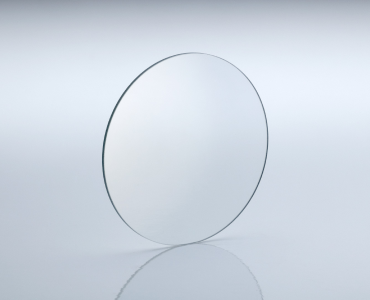
Fe doped LT Wafers
Curie Temp: 603±2℃
Cutting Angle: X/Y/Z/X112Y/Y36/Y42/Y48/etc
Diameter/size: 3”/4”/6" LT wafer
Tol(±): <0.20 mm
Thickness: 0.18 ~ 0.5mm or more
Primary Flat: 22mm /32mm /42.5mm /57.5mm
Our abundance experience at growing and mass production for SAW grade Lithium Tantalate. We are equipped with advanced facilities at Crystal growing, wafer lapping, polishing and checking, all finished products are passed at Testing of curie Temp and QC inspection.
Our abundance experience at growing and mass production for SAW grade Lithium Tantalate. We are equipped with advanced facilities at Crystal growing, wafer lapping, polishing and checking, all finished products are passed at Testing of curie Temp and QC inspection.
Our R&D is active at developing and researching from new material to finished products at all kinds of Fe doped wafers & electronic components.
| Material | LiTaO3 wafers(White or Black &Fe doped) | |
| Curie Temp | 603±2℃ | |
| Cutting Angle | X/Y/Z/X112Y/Y36/Y42/Y48/etc | |
| Diameter/size | 3”/4”/6″ LT wafer | |
| Tol(±) | <0.20 mm | |
| Thickness | 0.18 ~ 0.5mm or more | |
| Primary Flat | 22mm /32mm /42.5mm /57.5mm | |
| LTV (5mmx5mm) | <1µm | |
| TTV | <3µm | |
| Bow | -30<bow<30 | |
| Warp | <40µm | |
| PLTV(<0.5um) | ≥95%(5mm*5mm) | |
| Orientation Flat | All available | |
| Surface Type | Single Side Polished /Double Sides Polished | |
| Polished side Ra | <0.5nm | |
| Back Side Criteria | General is 0.2-0.5µm or as customized | |
| Edge Criteria | R=0.2mm or Bullnose | |
| Fe doped | Fe doped for saw grade LN< wafers | |
| Wafer Surface Criteria | Transmissivity | general:5.9×10⁻¹¹<s<2.0*10-10 at 25℃ |
| Contamination, | None | |
| Particles ¢>0.3 µ m | <= 30 | |
| Scratch , Chipping | None | |
| Defect | No edge cracks, scratches, saw marks, stains | |
| Packaging | Qty/Wafer box | 25pcs per box |
Our Ordering Process
Send us your request with detailed specifications
Receive a commercial offer with terms and costs
After your approval, we handle manufacturing, quality control, and shipping
📦 Shipping
3-5 days in EU, from 10 days to USA
💳 Payment methods
Cash, Bank Transfer, Cards (Visa, Mastercard, Amex, Discover) and PayPal
💬 Questions?
Contact us via WhatsApp, phone, live chat or email
