Lithium Niobate on Insulator Substrates LNOI
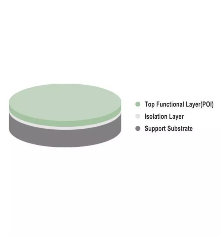
Isolation Layer
Support substrate
Lithium Niobate Thin Films on Insulator is kind of POI (Piezoelectric on Insulator) wafer. It’s stacked sequence structure is made of support substrates that can be silicon, quartz, fused silica, sapphire or LN wafer, the interlayer is thermal oxide SiO2 that works as insulator and lithium niobate film is the functional layer above the insulation layer.
POI /LNOI engineered substrates enable the design of filters with high quality factor, large bandwidth, very low temperature sensitivity and low insertion loss with a simple device manufacturing technology. These wafers are developed and used for high-speed modulators, high Q factor SAW devices, IR-detectors, THz devices.
We work with our strategical partner who has experienced at technology of smart cut and wafer bonding and supply with important Piezoelectric layer on LN/LT from the sizes of 3” 4” 6” up to 8” to build the special wafer with multilayered structure.
Specifications For LNOI
|
Layers |
Parameters |
Specifications |
|||
| Top Functional Layer | Material | Lithium Niobate Lithium Tantanlate | |||
| Diameter | 3″ | 4″ | 6″ | 8″ | |
| Surface orientation | X-cut or per request | ||||
| Primary flat oritentation | per request | deg(°) | |||
| Secondary flat orientation | per request | ||||
| Film Thickness average thickness | 300-600 | nm | |||
| Front side /face roughness | Optical polished | ||||
| Isolation Layer | Buried Oxide avg thickness | 4600 | 4700 | 4800 | nm |
| Buried Oxide thickness uniformity | -5 | 0 | 5 | % | |
| Support substrate | Material | SI/LN/SAPPHIRE/QUARTZ/ETC | |||
| Diameter | 3″ | 4″ | 6″ | 8″ | |
| Support layer total thickness | 525 | 525 | 625 | 725 | |
| Device growth method | CZ | CZ | ZVD | hydrothermal | |
| Device orientation | {100} | 0.5 | deg(°) | ||
| Device doping type | N | N | |||
| Device dopant | Phos | ||||
| Surface finish | 10 | nm | |||
Our Ordering Process
Send us your request with detailed specifications
Receive a commercial offer with terms and costs
After your approval, we handle manufacturing, quality control, and shipping
📦 Shipping
3-5 days in EU, from 10 days to USA
💳 Payment methods
Cash, Bank Transfer, Cards (Visa, Mastercard, Amex, Discover) and PayPal
💬 Questions?
Contact us via WhatsApp, phone, live chat or email

