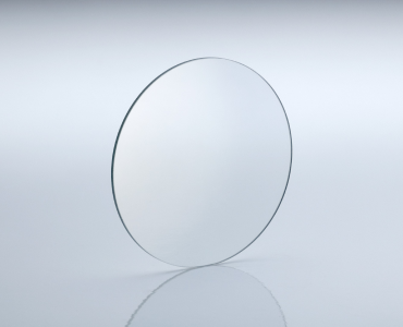
SAW Grade Lithium Niobate Wafers
Curie Temp: 1142±2.0℃
Cutting Angle: X/Y/Z/Y36/Y41/Y64/Y128/etc
Diameter/size: 3”/4”/6"LN wafer & 8"under R/D
Tol(±): <0.20 mm
Thickness: 0.18 ~ 0.5mm or more
Primary Flat: 22mm /32mm /42.5mm /57.5mm
Lithium Niobate (LiNbO3) is a useful optoelectronic material. The material not only has unique piezoelectric, optical and photoelastic properties, but also has good mechanical and chemical stability. Its combination of excellent electro-optic, acoustooptic and nonlinear optical properties makes it an attractive material in integrated optics.
CQT provides up to 6″ diameter, single crystal Optical grade LN material with reduced impurity levels. Other specifications can be provided are doped wafers: Er:LN, MgO:LN and Fe:LN.
The most used SAW orientations are YZ-cut and 128°Y-cut, best fit for television transmission and reception signal processing. The 128°Y-cut with X propagation is said to have the lowest spurious signal level.
Lithium Niobate (LN) is a ferroelectric material with excellent electro-optic, nonlinear, and piezoelectric properties. Lithium niobate crystals are important materials for optical waveguides, mobile phones, piezoelectric sensors, optical modulators and various other linear and non-linear optical applications.
The largest use of Lithium Niobate (LN) is in SAW devices used in telecommunication devices. When voice communication and data communication are performed, SAW devices such as SAW filters and SAW duplexers are mounted in communication devices as filters for preventing noise and interference. Lithium Niobate (LN) crystals are also used in optical applications.
| Material | LiNbO3 wafers (White or Black) | |
| Curie Temp | 1142±2.0℃ | |
| Cutting Angle | X/Y/Z/Y36/Y41/Y64/Y128/etc | |
| Diameter/size | 3”/4”/6″LN wafer & 8″under R/D | |
| Tol(±) | <0.20 mm | |
| Thickness | 0.18 ~ 0.5mm or more | |
| Primary Flat | 22mm /32mm /42.5mm /57.5mm | |
| LTV (5mmx5mm) | <1µm | |
| TTV | <3µm | |
| Bow | -30<bow<30 | |
| Warp | <40µm | |
| PLTV(<0.5um) | ≥95%(5mm*5mm) | |
| Orientation Flat | All available | |
| Surface Type | Single Side Polished /Double Sides Polished | |
| Polished side Ra | <0.5nm | |
| Back Side Criteria | General is 0.2-0.5µm or as customized | |
| Edge Criteria | R=0.2mm or Bullnose | |
| Wafer Surface Criteria | Transmissivity | general:5.9×10⁻¹¹<s<2.0*10-10 at 25℃ |
| Contamination, | None | |
| Particles ¢>0.3 µ m | <= 30 | |
| Scratch , Chipping | None | |
| Defect | No edge cracks, scratches, saw marks, stains | |
| Packaging | Qty/Wafer box | 25pcs per box |
Our Ordering Process
Send us your request with detailed specifications
Receive a commercial offer with terms and costs
After your approval, we handle manufacturing, quality control, and shipping
📦 Shipping
3-5 days in EU, from 10 days to USA
💳 Payment methods
Cash, Bank Transfer, Cards (Visa, Mastercard, Amex, Discover) and PayPal
💬 Questions?
Contact us via WhatsApp, phone, live chat or email
