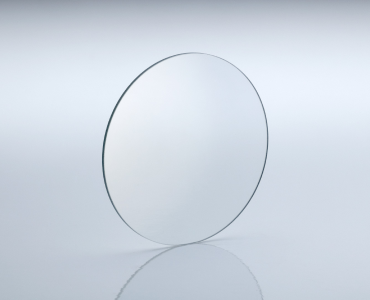
Silicon Wafer Blank
Dimension: Dia. 90.00mm
Thickness: 6.20mm
Tolerance : +/-0.10mm
Silicon wafer blanks are foundational components in the semiconductor industry, serving as the backbone for a wide range of electronic devices. These wafers are crafted from hyperpure silicon, which is meticulously processed to achieve the high levels of purity and precision required for modern electronics. By selectively doping silicon with trace amounts of elements like boron, gallium, phosphorus, or arsenic, manufacturers can fine-tune its electrical properties to meet specific application needs. This adaptability makes silicon wafer blanks indispensable in industries such as computing, microelectronics, and telecommunications.
Technical Specifications of Silicon Wafer Blanks
Our silicon wafer blanks are engineered to deliver exceptional performance and reliability, with key specifications that ensure consistency and quality:
- Transmission Range: 1.2 to 7.0 microns, making them suitable for applications across infrared and visible light spectra.
- Density: 2.329 g/cm³, providing a lightweight yet durable base for semiconductor devices.
- Refractive Index: 3.4223 at 5 microns, ensuring precise control over light transmission and optical performance.
- Melting Point: 1420°C, allowing the material to withstand extreme temperatures during fabrication and operation.
- Surface Finish: Fine grinding ensures a smooth and uniform surface, while optional felt polishing enhances optical clarity.
- Cylindrical Surface: Available with fine grinding or felt polishing to meet specific application requirements.
- Chamfer/Bevel: 0.2-0.3mm, reducing the risk of chipping or damage during handling.
- Parallelism: Less than 3 arc minutes, ensuring precise alignment for layered semiconductor structures.
- Irregularity: Less than 2 fringes, guaranteeing minimal distortion and consistent performance.
Advantages of Silicon Wafer Blanks
Silicon wafer blanks offer numerous advantages that make them the preferred choice for semiconductor manufacturing:
- Hyperpure Quality: The use of hyperpure silicon ensures minimal impurities, enabling reliable and predictable electrical performance.
- Customizable Properties: Doping with elements like boron or phosphorus allows precise control over conductivity and other electrical characteristics.
- High Thermal Stability: With a melting point of 1420°C, these wafers can endure the high-temperature processes involved in semiconductor fabrication.
- Optical Clarity: The fine grinding and optional felt polishing provide excellent surface quality, enhancing light transmission and reducing scattering.
- Dimensional Precision: Tight tolerances in parallelism and irregularity ensure compatibility with advanced lithography and etching techniques.
- Versatility: Suitable for a wide range of applications, from integrated circuits to photovoltaic cells and optoelectronic devices.
Applications of Silicon Wafer Blanks
Silicon wafer blanks are integral to numerous industries and technologies, including:
- Computer and Microelectronics: Used as substrates for integrated circuits (ICs) and microprocessors, powering everything from smartphones to supercomputers.
- Photovoltaics: Serve as the foundation for solar cells, converting sunlight into electricity with high efficiency.
- Telecommunications: Enable the development of advanced optoelectronic devices, such as lasers and photodetectors.
- Research and Development: Provide a reliable platform for experimenting with new materials and semiconductor designs.
- Automotive Electronics: Support the growing demand for sensors and control systems in modern vehicles.
Technical Specifications Table
| Property | Specification |
|---|---|
| Transmission Range | 1.2 to 7.0 microns |
| Density | 2.329 g/cm³ |
| Refractive Index | 3.4223 @ 5um |
| Melting Point | 1420°C |
| Surface | Fine Grinding |
| Cylindrical Surface | Fine Grinding / Felt Polish |
| Chamfer/Bevel | 0.2-0.3mm |
| Parallelism | < 3 arc minutes |
| Irregularity | < 2 fringes |
Silicon wafer blanks are the cornerstone of modern semiconductor technology, enabling advancements in computing, energy, and telecommunications. Their combination of hyperpure quality, customizable electrical properties, and precise dimensional tolerances makes them ideal for a wide range of applications. Whether used in cutting-edge microprocessors, efficient solar cells, or advanced optoelectronic devices, silicon wafer blanks deliver unmatched performance and reliability. With rigorous quality control and customizable options, our silicon wafer blanks ensure that your projects meet the highest standards of innovation and functionality. Embrace the power of silicon technology to drive your next breakthrough in electronics and beyond.
* Curve of Silion
![]()
Picture shown is a Silion blank, with D90mm and T6.20mm. Also produce other size and specification of Si wafer, or other high precision windows fabricated from several other substrates for use in a large variety of laser and industrial applications.
Our Ordering Process
Send us your request with detailed specifications
Receive a commercial offer with terms and costs
After your approval, we handle manufacturing, quality control, and shipping
📦 Shipping
3-5 days in EU, from 10 days to USA
💳 Payment methods
Cash, Bank Transfer, Cards (Visa, Mastercard, Amex, Discover) and PayPal
💬 Questions?
Contact us via WhatsApp, phone, live chat or email
